From: Andreas Robinson (sleeper75se_at_yahoo.se)
Date: 2002-01-30 12:52:00
--- In buildcheapeeg_at_yahoogroups.com, "Jim Meissner"
<jpmeissner_at_mindspring.com> wrote:
>Eventually I found out that some smart production
>worker gotten an award for saving 3 feet of heavy
>wire that just ran from the front to the back and
>right back again. That extra wire was part of a
>star ground system and very important!
Hi Jim,
your story clearly shows that sometimes it is stupid
being clever. :-)
> I don't know what all the parts are, but on a quick
> inspection the way you have it looks correct.
> You should look at it from the star ground concept
> and see.
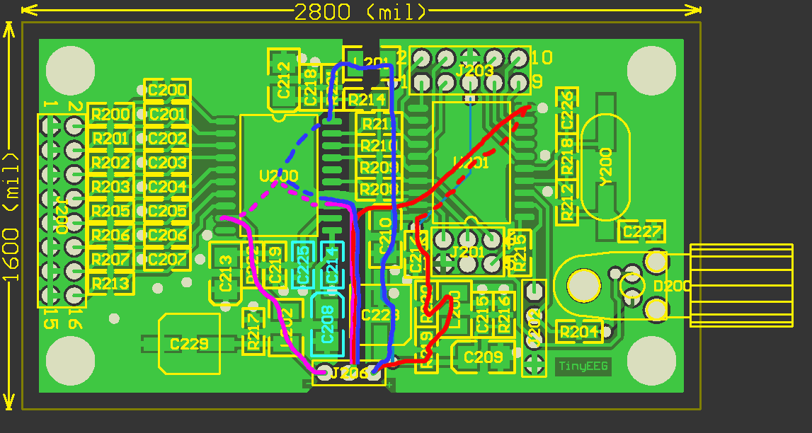
The power topology of the ADC-board is sort of
star-groundish. I've attached an image that shows my
analysis, please take a look at it.
I have traced the main power current-loops:
Purple is negative ADC power (VADC-)
Blue is positive ADC power (VADC+)
Red is MCU power (VMCU)
A quick listing of what all parts do:
The three parts colored in light blue, encircled by
the purple line, is the VREF decoupling.
Most of the rest is power decoupling and filtering.
>From this image I conclude that it probably is a good
idea to put a trace near GND on J206 (bottom, center)
to the ground plane to the right. That should reduce
the loops caused by VADC+ and VMCU.
I don't think it is good to do the same for the left
side, as that would cause the return current for VADC-
to run directly under the VREF decoupling, injecting
noise into VREF. Of two evils, the lesser one is to
let VADC- run in a loop, as it does now. It is mostly
covered by ground plane on the bottom side anyway.
What do you think, is my analysis correct?
> > I've managed to cut the costs a bit.
>
> This is not the time for that!
>
> Let me state my opinion about price again. FIRST
> make something that works, THEN re-evaluate the
> design and possibly give people some cost options.
Too late. :-) Actually, most of the savings does
*not* come from changing function, but rather from
picking the right (passive) parts and playing a bit
with the filter. Browsing Digikey.com without a
paper-catalog is a real pain, their search system is
close to worthless and the pricing policy is sometimes
a bit illogical.
> Please get some hardware working. It looks real
> close. Let me know if I can help.
It *is* very close now. Just some layout tweaks, then
we're set to go!
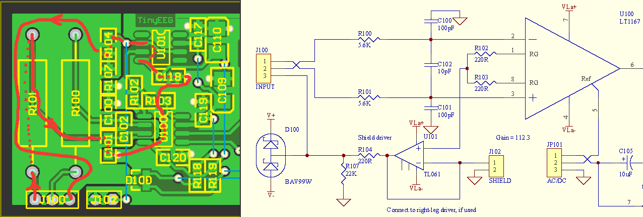
Ok, I have a question regarding the input stage. The
second attachment shows the preamplifier, both as
PCB-layout and the schematic for it.
Right now, the 100pF RF-chokes are connected to
ground, but I'm wondering if that is such a good idea.
In the attachment, I have traced the route the RF
would have to take, assuming it wants to return to the
shield.
It is not a pretty sight!
1. The disturbance enters through the electrode
connector to the left and passes through the
ESD-protection resistor R100.
2. Then it is diverted by the 100pF capacitor to
ground, where it proceeds directly under the
instrumentation amplifier chip U100 to a decoupling
capacitor for the shield driver U101.
3. It enters U101 through the negative power rail and
exits again through its output,
4. Then it passes through R104 before it dives into
the shield plane, where it has to take the scenic tour
before leaving the board.
Assuming the trace is correct: Yuck! :-)
My question: Is it?
Should I connect the 100pF caps to the shield driver
output instead? Then the RF currents would leave
before traversing any other parts. (By the way: as you
know, if someone chooses to not use the shield driver,
the shield is connected to ground instead.)
Regards,
Andreas
PS. To all modem users: Sorry for the heavy payload
(85k). DS.
_____________________________________________________
Hitta snörapporter...
frĺn 500 olika skidorter i Europa
pĺ http://se.snow.yahoo.com


This archive was generated by hypermail 2.1.4 : 2002-07-27 12:28:37 BST